- 您现在的位置:买卖IC网 > Sheet目录1214 > EVAL-ADM1166TQEBZ (Analog Devices Inc)BOARD EVAL FOR ADM1166TQ
�� ��
��
��ADM1166�
�OUTPUTS�
�SUPPLY� SEQUENCING� THROUGH� CONFIGURABLE�
�OUTPUT� DRIVERS�
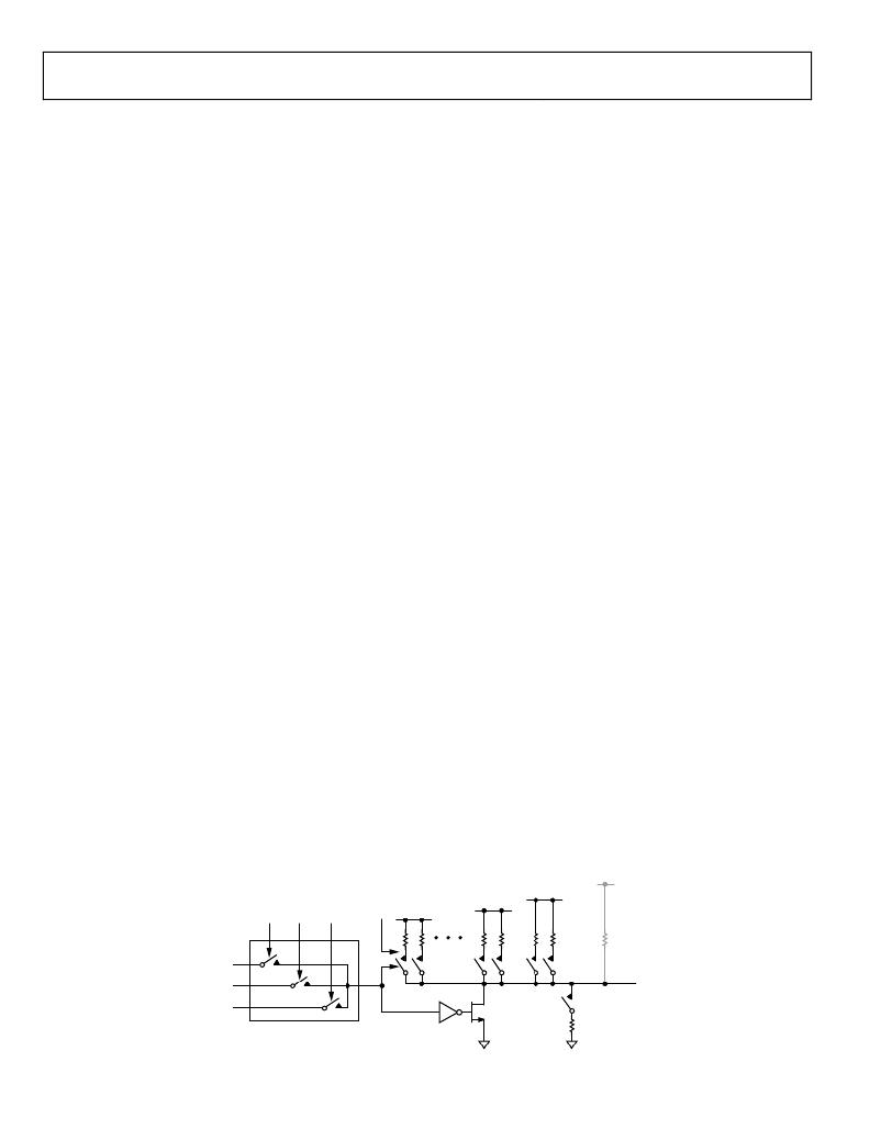
�Supply� sequencing� is� achieved� with� the� ADM1166� using� the�
�programmable� driver� outputs� (PDOs)� on� the� device� as� control�
�The� data� driving� each� of� the� PDOs� can� come� from� one� of� three�
�sources.� The� source� can� be� enabled� in� the� PDOxCFG� configu-�
�ration� register� (see� the� AN-698� Application� Note� for� details).�
�The� data� sources� are� as� follows:�
�signals� for� supplies.� The� output� drivers� can� be� used� as� logic�
�enables� or� as� FET� drivers.�
�?�
�?�
�Output� from� the� SE.�
�Directly� from� the� SMBus.� A� PDO� can� be� configured� so� that�
�The� sequence� in� which� the� PDOs� are� asserted� (and,� therefore,�
�the� supplies� are� turned� on)� is� controlled� by� the� sequencing� engine�
�(SE).� The� SE� determines� what� action� is� taken� with� the� PDOs,�
�based� on� the� condition� of� the� ADM1166� inputs.� Therefore,� the�
�PDOs� can� be� set� up� to� assert� when� the� SFDs� are� in� tolerance,� the�
�correct� input� signals� are� received� on� the� VXx� digital� pins,� and�
�no� warnings� are� received� from� any� of� the� inputs� of� the� device.�
�The� PDOs� can� be� used� for� a� variety� of� functions.� The� primary�
�function� is� to� provide� enable� signals� for� LDOs� or� dc-to-dc�
�converters� that� generate� supplies� locally� on� a� board.� The� PDOs�
�can� also� be� used� to� provide� a� PWRGD� signal,� when� all� the� SFDs�
�are� in� tolerance,� or� a� RESET� output� if� one� of� the� SFDs� goes� out�
�of� specification� (this� can� be� used� as� a� status� signal� for� a� DSP,�
�FPGA,� or� other� microcontroller).�
�the� SMBus� has� direct� control� over� it.� This� enables� software�
�control� of� the� PDOs.� Therefore,� a� microcontroller� can� be�
�used� to� initiate� a� software� power-up/power-down� sequence.�
�?� On-chip� clock.� A� 100� kHz� clock� is� generated� on� the� device.�
�This� clock� can� be� made� available� on� any� of� the� PDOs.� It�
�can� be� used,� for� example,� to� clock� an� external� device� such�
�as� an� LED.�
�DEFAULT� OUTPUT� CONFIGURATION�
�All� of� the� internal� registers� in� an� unprogrammed� ADM1166�
�device� from� the� factory� are� set� to� 0.� Because� of� this,� the� PDOx� pins�
�are� pulled� to� GND� by� a� weak� (20� kΩ),� on-chip� pull-down� resistor.�
�As� the� input� supply� to� the� ADM1166� ramps� up� on� VPx� or� VH,�
�all� PDOx� pins� behave� as� follows:�
�The� PDOs� can� be� programmed� to� pull� up� to� a� number� of� different�
�options.� The� outputs� can� be� programmed� as� follows:�
�?�
�?�
�Input� supply� =� 0� V� to� 1.2� V.� The� PDOs� are� high� impedance.�
�Input� supply� =� 1.2� V� to� 2.7� V.� The� PDOs� are� pulled� to� GND�
�?�
�Open� drain� (allowing� the� user� to� connect� an� external�
�by� a� weak� (20� kΩ),� on-chip� pull-down� resistor.�
�pull-up� resistor).�
�?�
�Supply� >� 2.7� V.� Factory-programmed� devices� continue� to�
�?�
�?�
�?�
�?�
�?�
�?�
�Open� drain� with� weak� pull-up� to� V� DD� .�
�Open� drain� with� strong� pull-up� to� V� DD� .�
�Open� drain� with� weak� pull-up� to� VPx.�
�Open� drain� with� strong� pull-up� to� VPx.�
�Strong� pull-down� to� GND.�
�Internally� charge� pumped� high� drive� (12� V,� PDO1� to�
�pull� all� PDOs� to� GND� by� a� weak� (20� kΩ),� on-chip� pull-down�
�resistor.� Programmed� devices� download� current� EEPROM�
�configuration� data,� and� the� programmed� setup� is� latched.� The�
�PDO� then� goes� to� the� state� demanded� by� the� configuration.�
�This� provides� a� known� condition� for� the� PDOs� during�
�power-up.�
�PDO6� only).�
�The� last� option� (available� only� on� PDO1� to� PDO6)� allows� the�
�user� to� directly� drive� a� voltage� high� enough� to� fully� enhance� an�
�external� N-FET,� which� is� used� to� isolate,� for� example,� a� card-�
�side� voltage� from� a� backplane� supply� (a� PDO� can� sustain� greater�
�than� 10.5� V� into� a� 1� μA� load).� The� pull-down� switches� can� also�
�be� used� to� drive� status� LEDs� directly.�
�The� internal� pull-down� can� be� overdriven� with� an� external� pull-up�
�of� suitable� value� tied� from� the� PDOx� pin� to� the� required� pull-up�
�voltage.� The� 20� k� resistor� must� be� accounted� for� in� calculating�
�a� suitable� value.� For� example,� if� PDOx� must� be� pulled� up� to� 3.3� V,�
�and� 5� V� is� available� as� an� external� supply,� the� pull-up� resistor�
�value� is� given� by�
�3.3� V� =� 5� V� ×� 20� kΩ/(� R� UP� +� 20� kΩ)�
�Therefore,�
�R� UP� =� (100� kΩ� ?� 66� kΩ)/3.3� V� =� 10� kΩ�
�VFET� (PDO1� TO� PDO6� ONLY)�
�V� DD�
�VP4�
�SE� DATA�
�SMBus� DATA�
�CFG4� CFG5� CFG6�
�SEL�
�VP1�
�PDO�
�CLK� DATA�
�Figure� 25.� Programmable� Driver� Output�
�Rev.� 0� |� Page� 16� of� 32�
�发布紧急采购,3分钟左右您将得到回复。
相关PDF资料
EVAL-ADM1168LQEBZ
BOARD EVAL FOR ADM1168LQ
EVAL-ADM1170EBZ
BOARD EVALUATION FOR ADM1170
EVAL-ADM1171EBZ
BOARD EVALUATION FOR ADM1171
EVAL-ADM1172EBZ
BOARD EVALUATION FOR ADM1172
EVAL-ADM1175EBZ
BOARD EVALUATION FOR ADM1175
EVAL-ADM1176EBZ
BOARD EVALUATION FOR ADM1176
EVAL-ADM1177EBZ
BOARD EVALUATION FOR ADM1177
EVAL-ADM1178EBZ
BOARD EVALUATION FOR ADM1178
相关代理商/技术参数
EVAL-ADM1168LQEBZ
功能描述:BOARD EVAL FOR ADM1168LQ RoHS:是 类别:编程器,开发系统 >> 评估演示板和套件 系列:* 标准包装:1 系列:- 主要目的:电信,线路接口单元(LIU) 嵌入式:- 已用 IC / 零件:IDT82V2081 主要属性:T1/J1/E1 LIU 次要属性:- 已供物品:板,电源,线缆,CD 其它名称:82EBV2081
EVAL-ADM1169LQEBZ
功能描述:BOARD EVAL FOR ADM1169LQ RoHS:是 类别:编程器,开发系统 >> 评估演示板和套件 系列:Super Sequencer® 标准包装:1 系列:PSoC® 主要目的:电源管理,热管理 嵌入式:- 已用 IC / 零件:- 主要属性:- 次要属性:- 已供物品:板,CD,电源
EVAL-ADM1170EBZ
功能描述:BOARD EVALUATION FOR ADM1170 RoHS:是 类别:编程器,开发系统 >> 评估演示板和套件 系列:- 标准包装:1 系列:- 主要目的:电信,线路接口单元(LIU) 嵌入式:- 已用 IC / 零件:IDT82V2081 主要属性:T1/J1/E1 LIU 次要属性:- 已供物品:板,电源,线缆,CD 其它名称:82EBV2081
EVAL-ADM1171EBZ
功能描述:BOARD EVALUATION FOR ADM1171 RoHS:是 类别:编程器,开发系统 >> 评估演示板和套件 系列:- 标准包装:1 系列:- 主要目的:电信,线路接口单元(LIU) 嵌入式:- 已用 IC / 零件:IDT82V2081 主要属性:T1/J1/E1 LIU 次要属性:- 已供物品:板,电源,线缆,CD 其它名称:82EBV2081
EVAL-ADM1172EBZ
功能描述:BOARD EVALUATION FOR ADM1172 RoHS:是 类别:编程器,开发系统 >> 评估演示板和套件 系列:- 标准包装:1 系列:- 主要目的:电信,线路接口单元(LIU) 嵌入式:- 已用 IC / 零件:IDT82V2081 主要属性:T1/J1/E1 LIU 次要属性:- 已供物品:板,电源,线缆,CD 其它名称:82EBV2081
EVAL-ADM1175EBZ
功能描述:BOARD EVALUATION FOR ADM1175 RoHS:是 类别:编程器,开发系统 >> 评估演示板和套件 系列:- 标准包装:1 系列:- 主要目的:电信,线路接口单元(LIU) 嵌入式:- 已用 IC / 零件:IDT82V2081 主要属性:T1/J1/E1 LIU 次要属性:- 已供物品:板,电源,线缆,CD 其它名称:82EBV2081
EVAL-ADM1176EBZ
功能描述:BOARD EVALUATION FOR ADM1176 RoHS:是 类别:编程器,开发系统 >> 评估演示板和套件 系列:- 标准包装:1 系列:- 主要目的:电信,线路接口单元(LIU) 嵌入式:- 已用 IC / 零件:IDT82V2081 主要属性:T1/J1/E1 LIU 次要属性:- 已供物品:板,电源,线缆,CD 其它名称:82EBV2081
EVAL-ADM1177EBZ
功能描述:BOARD EVALUATION FOR ADM1177 RoHS:是 类别:编程器,开发系统 >> 评估演示板和套件 系列:- 标准包装:1 系列:- 主要目的:电信,线路接口单元(LIU) 嵌入式:- 已用 IC / 零件:IDT82V2081 主要属性:T1/J1/E1 LIU 次要属性:- 已供物品:板,电源,线缆,CD 其它名称:82EBV2081